
| C. Scott home | Back to projects page | MAS863 home |
On this page we will discuss the power electronics needed for our EDM machine. The basic mechanism of electrical discharge machining is a controlled spark between the electrode and the workpiece. This part of the electronic design generates the waveforms necessary to induce the spark. We will start by describing the fundamental mechanisms of EDM which dictate the voltage, current, and frequency needed, then show a very simple circuit satifying these requirements before describing its limitations and addressing these with an improved circuit.
I spent some time in the library reading all the material on EDM that I could find. I will attempt to give a bibliographical reference for each essential fact I note below, to allow the curious reader to duplicate my research.
| Electrode gap | Breakdown Voltage |
|---|---|
| .001" | 10V |
| .002" | 176V |
| .003" | 220V |
| .004" | 295V |
| .005" | 440V |
| .006" | 395V |
| .007" | 562V |
| .008" | — |
| .009" | — |
| .010" | — |
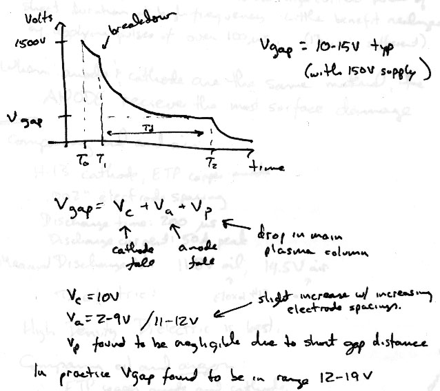
The figure below (from [DOR]) shows a typical waveform during an EDM spark:
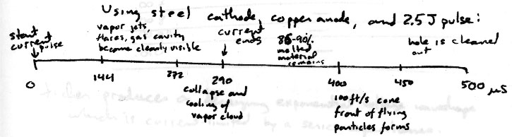
This figure shows the timescale of an EDM discharge:
We will design our EDM to generate 100us pulses of 50A at either 150V or 300V peak-to-peak. This should be sufficient for operation at gaps up to .002" (for 150V) or .004" (for 300V). We will be driving the machine from a standard 15A edison circuit (the kind you have in your home), so our ideal duty cycle will be around 33% to keep the average current draw down to 15A.
The following simple circuit is the one described in [LAN]. It generates 60V at 5A, which is sufficient for light-duty EDM.
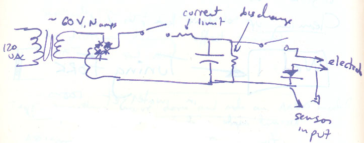
The power delivered to the electrodes is limited by the capacity of the transformer at the input, and the voltage (60V) is a little low by EDM standards. Omitting the transformer increases voltage to about 150V and allows us to suck up as much current as a standard wall outlet will give (15A):
![]()
The main drawback with a circuit of this type is the large amount of power dissipated in the current-limiting resistors (R1 in the above; both circuits as drawn are also missing additional current-limiting resistors in series with the electrode). Current-limiting is necessary to protect the switching transistors and other components, which can only handle a limited amount of current. But the passive approach requires 1700W to be dissipated in R1 and about 2000kW to be dissipated in the electrode current limiting resistor. Resistors that can handle this amount of power are expensive --- DigiKey lists 1000W resistors for over $100 each, and we'd need 4 of them!
Instead of passively limiting our current, we can use an active circuit to do so. The basic idea is that we will watch the current flowing through the circuit, and if it ever exceeds our desired limit value, we will flip a switch and turn the source off. When the current falls back down to an acceptable value, we'll turn the source back on. The on-and-off action will generate a little bit of ripple in the output current, but if we keep the frequency high enough the ripple should be reasonable.
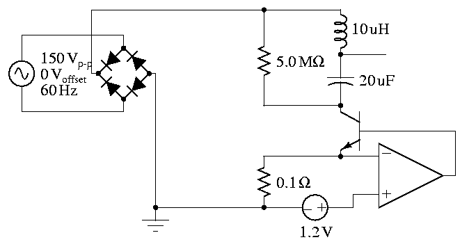
Our new circuit looks roughly like this:
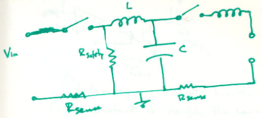
Instead of a series current-limiting resistor, we have only a very small "sense" resistor: the voltage across the sense resistor will tell us how much current is flowing through the loop. We add an inductor, L, to limit the rate of change of the current, to ensure that our switches are fast enough to restrict sudden rises in current.
For background, here is a simple RLC circuit and how it behaves:
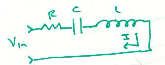
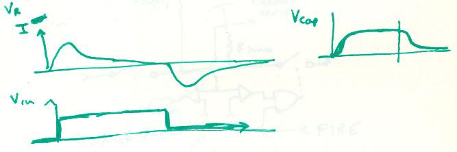
Note that the slope of I is limited.
Here is our current-limiting circuit, fleshed out:
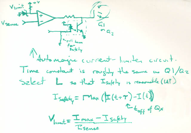
The output of the comparator feeds into the RLC network like this:
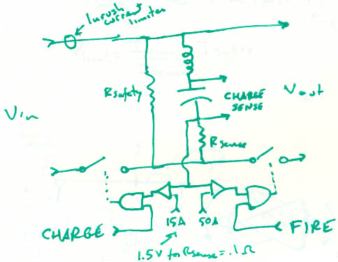
Here's a cleaned-up version of the first stage.
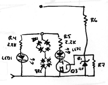
We need some feedback on whether we're sparking correctly or have an open or short condition in order to maintain the electrode gap distance properly. The following circuit provides this. The LEDs in the circuit are inputs to optoisolators. Note the use of diodes as impromptu voltage regulators.
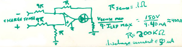
We'd also like to be able to sense the current capacitor voltage to allow low-voltage pulses. This circuit does that. Again, the LED is input to an analog-input optoisolator; the op-amp circuit maintains the current through the LED to be proportional to the voltage drop across the capacitor.
Here's the completed schematic for the power front-end:

The full schematic fleshes out the rough sketches above. The IGBT power transistors require a special gate drive circuit, the IR2108; in this application we might need a charge pump (the ICM7555) to obtain a sustained gate drive voltage. All the power electronics are optoisolated from the control electronics. We've got a separate 15V supply to run the switching regulator control.
Updated! I've updated the schematic above to better regulate the current through the electrode gap. We need a catch diode to continue directing current (from the inductor) through the gap even when the voltage source (the power capacitor) is switched off. I also added an extra "boost" transistor to the circuit. If we initially turn this on, we'll get 50A or so of current flowing through the output inductor, although there will be no voltage across the gap. Switching the boost transistor off will cause the current to flow across the gap --- and the inductor will raise the voltage at the electrode to whatever level is necessary to make this happen. We potentially get quite a lot of voltage boost here, ensuring a good spark. The zener diode (MOSORB) across the boost transistor ensures that the voltage doesn't get high enough to toast the transistor. We needed to add another gate driver chip (the IR2117) to accomodate these changes.
Updated! (again) I've updated the schematic to reflect my most recent working version; in particular the old version was missing the Vsense input to the comparators (oops). I've also posted an email I recently wrote to Roger Cook, giving some more details on component specification and circuit operation.
Updated! (yet again) I posted some correspondence between Roger Cook and Grant Saviers regarding this design.
This schematic was drawn with XCircuit; the source file is edm-power.ps (yes, XCircuit uses PostScript as its native file format). From the schematic XCircuit generates a PCB-format netlist, edm-power.pcb.


|
Copyright © 2002 C. Scott Ananian. Verbatim copying and distribution is permitted in any medium, provided this notice is preserved. |
cananian@mit.edu |